
Get deeper into the Arduino craft by looking into a reference design. In here I will get into details with the basic arduino schematic diagram using one of their more popular development board, the Arduino UNO.
So what is an Arduino? It can basically mean two things:
One, it is an open-source hardware and software company that creates circuit boards that makes microcontrollers easier to use. Open-source means its source code and hardware design is freely available for anyone to modify. With the code and design free, public collaboration can develop the product way faster than any proprietary product. The only downside of giving the public access is that it gives birth to competition. It allows clones. This is the also the reason why we can only do a diagram analysis of Arduino, and not a Raspberry Pi.
Two and the more popular use of the term is that the board itself is called an Arduino.
There are a lot of tutorials for Arduino in the internet. Nearly all of them explains how to make it work but, how does it work? A good understanding of the hardware design will help you learn how to incorporate them on your machines, small-scale to large.
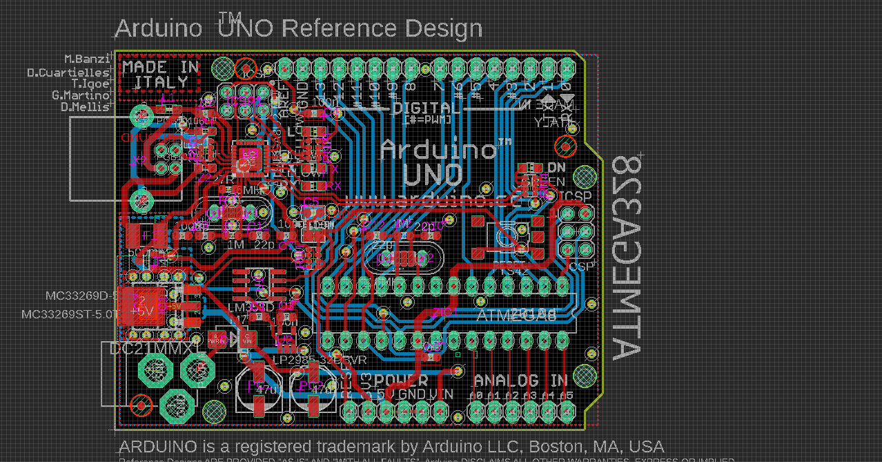
Here we have the schematic diagram of the latest revision of Arduino UNO. Don’t worry if you can’t see it much right now. We’ll chop it up after and analyze every section according to their function.

Components
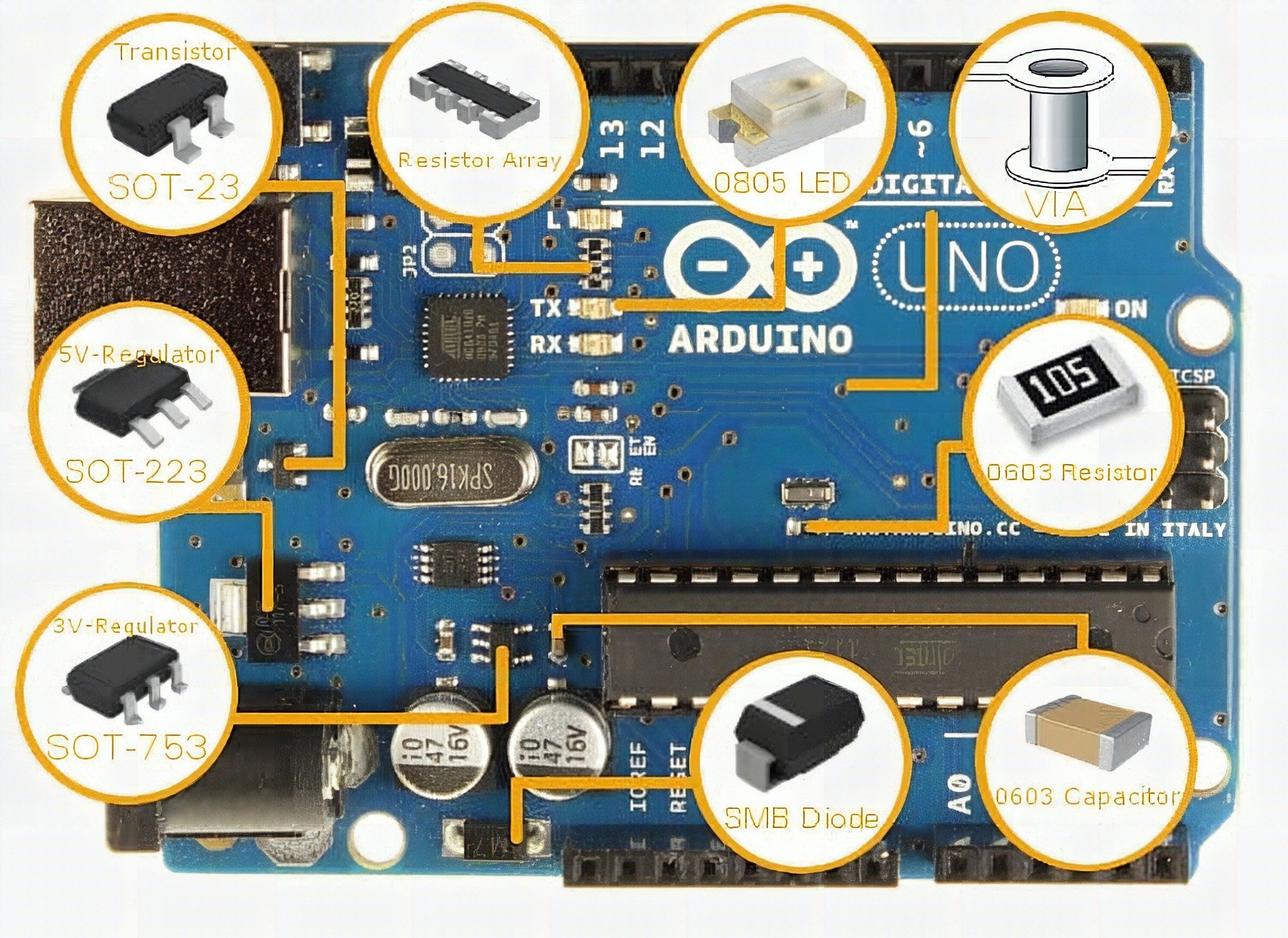
Here we can visibly identify each component on board, besides the obvious Atmega328P. Depending on the IC package, these components can appear differently. If you want to learn more about IC packages. Visit this SparkFun webpage.
We will divide the schematic diagram into four major sections: Power Supply, Main Microcontroller, USB bridge and lastly the Input and Output.
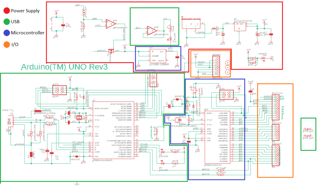
POWER SUPPLY

This section of the schematic diagram powers our Arduinos. For this, we can use either DC power supply or USB connection as a source. To trace how the circuit works, let us start with the 5V linear voltage regulator NCP1117ST50T3G. This regulator has a pretty straightforward function. It takes voltage input up to 20V and converts it to 5V. The Vin of this regulator is connected to the DC power supply via the M7 diode. This diode provides

reverse polarity protection, which means current can only flow from the power supply to the regulator and not the other way around. There are two kinds of capacitors used in this circuit. One, the polarized capacitors PC1 and PC2. They are used to filter supply noise. Two, the 100nF capacitor on the far right side acting as a decoupling capacitor. Decoupling capacitors “disconnects” circuit elements to reduce its effect on the rest of the circuit. Also, notice the +5V terminals circled in blue? You can see them around the schematic diagram. That is basically a connection. Designers often use these terminals so that they can fit their design in the least amount of pages. Labels like Vin and GND also works the same.
Choosing the Power Source
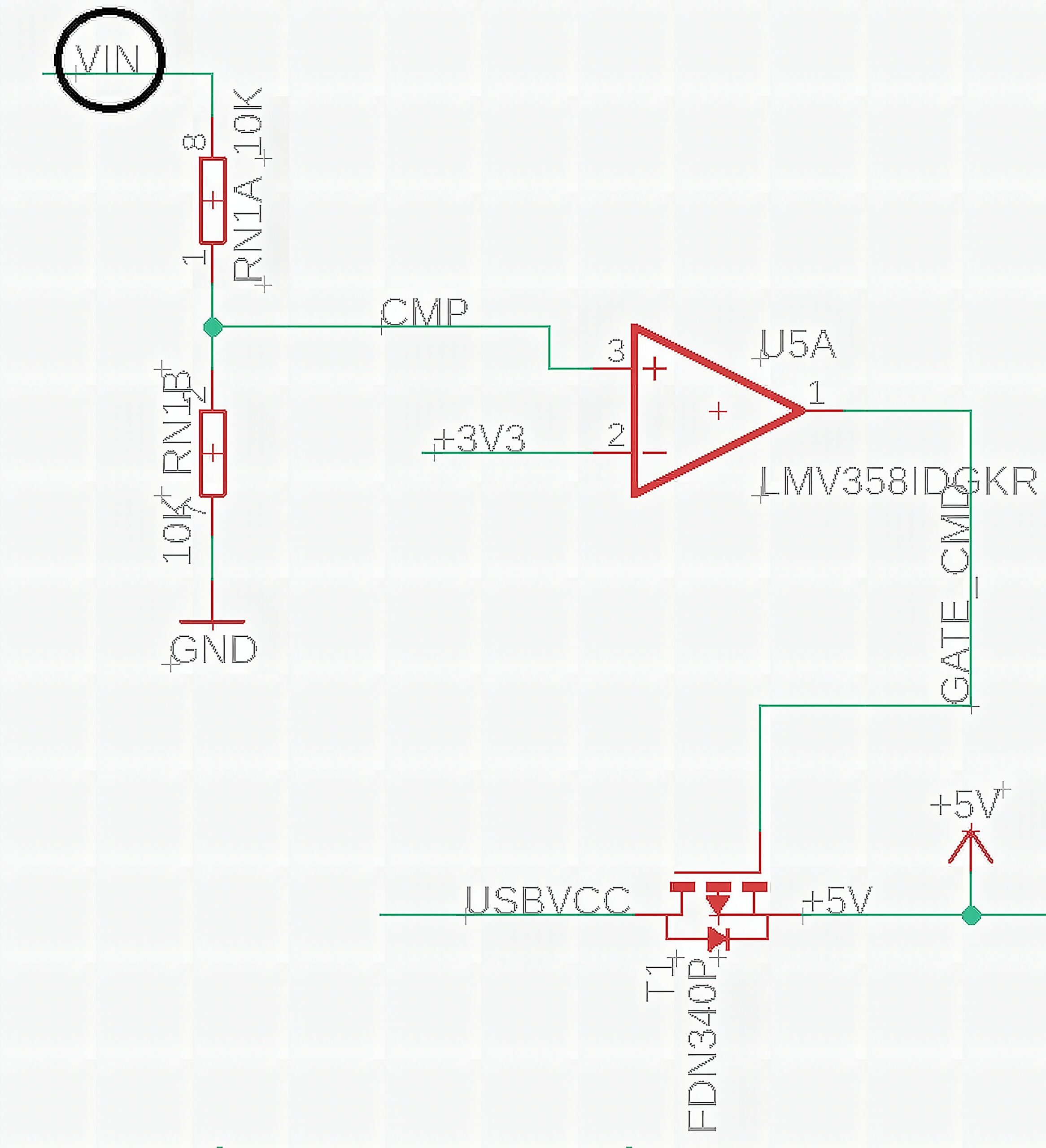
If you use the USB source, power will enter through the USBVCC section into a P-channel MOSFET FDN340P. Explaining briefly, MOSFETS are transistors that are normally closed (connected) until a certain amount of voltage triggers the gate. Consequently, triggering the MOSFET opens the transistor (disconnected). Using this characteristic, a comparator is connected to the gate terminal of the MOSFET to function as a switch mechanism. If you use the USB source, it will just power up the 3.3V regulator since the MOSFET is normally connected. If you plug a dc supply, the LMV358 op-amp will produce a high output triggering the gate of the MOSFET, disconnecting the USB source from the 3.3V regulator. So if both are plugged, the board will use the DC power supply.

The 5V terminal here indicates a connection to the circuit powered by the DC power supply earlier. This means that the 3.3V regulator is powered by whichever powers the circuit.
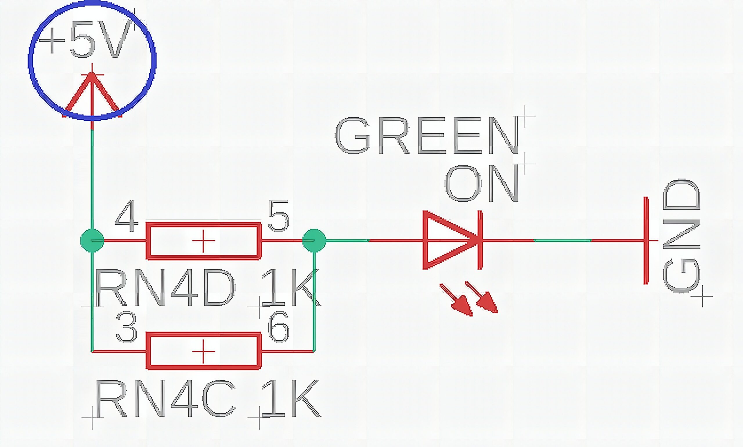
Lastly, the LED indicator circuit. Put simply, it lights the green LED up when it detects power from the 5V terminal.
MICROCONTROLLER
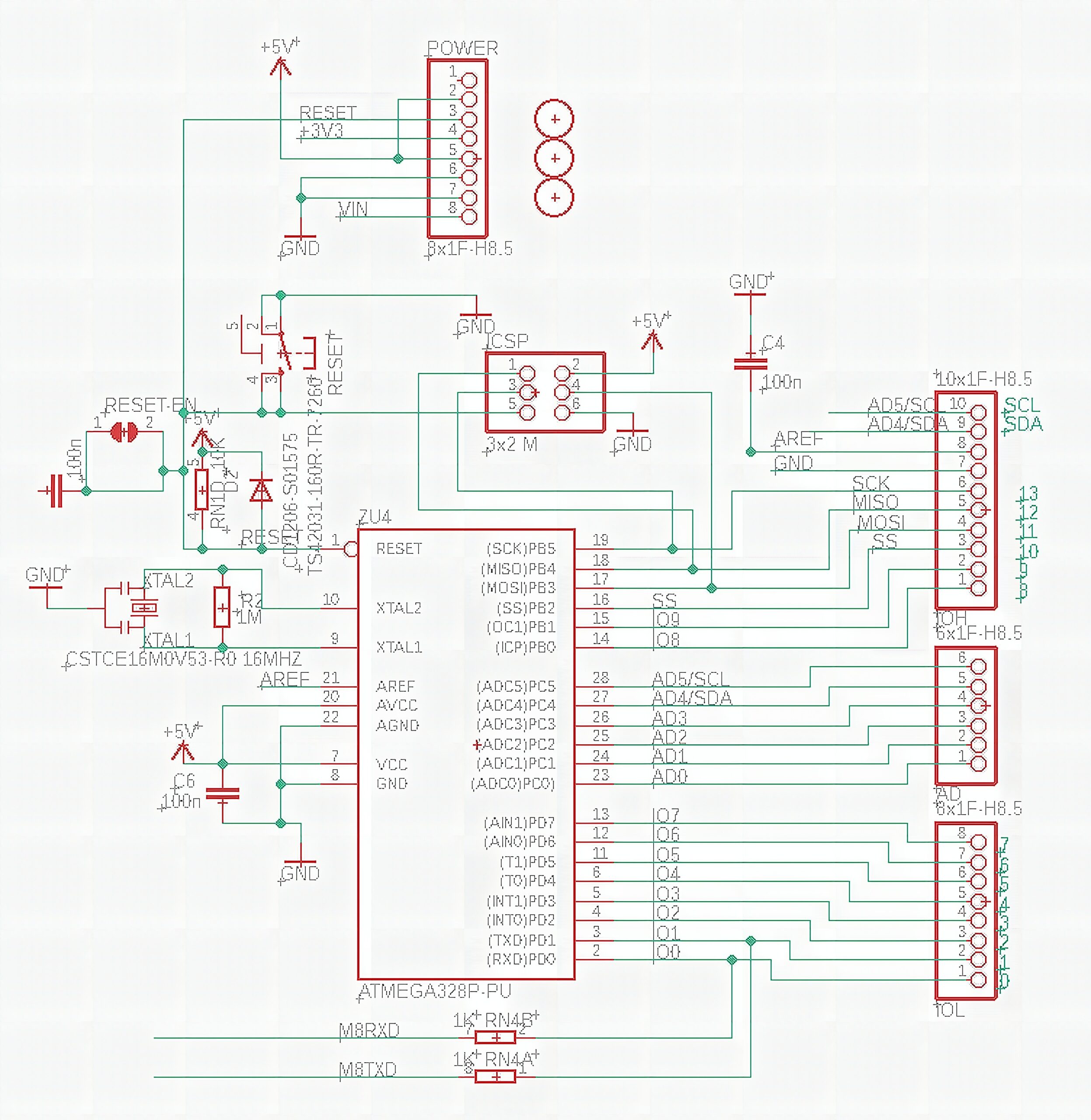
This section is the main microcontroller circuit of the Arduino UNO. It has the ATmega328P microcontroller. We won’t go into details with the microcontroller’s specs. The only thing you need to know is that it is an 8-bit device which means it can handle 8 data lines simultaneously.
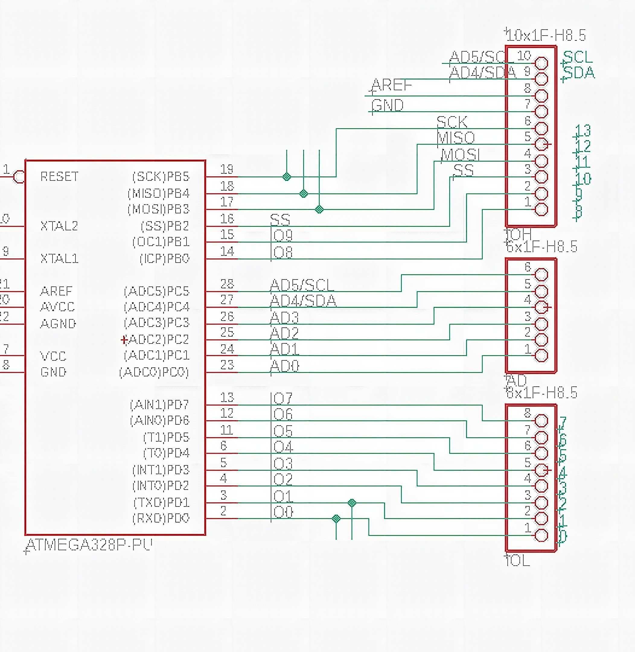
These three are the black headers you see on board. As you can see, the TX and RX from the ATmega16U2 are connected into pins 0 and 1. The IOL and IOH headers are for pins 0 to 13 in addition to the I2C pins, GND, and AREF.
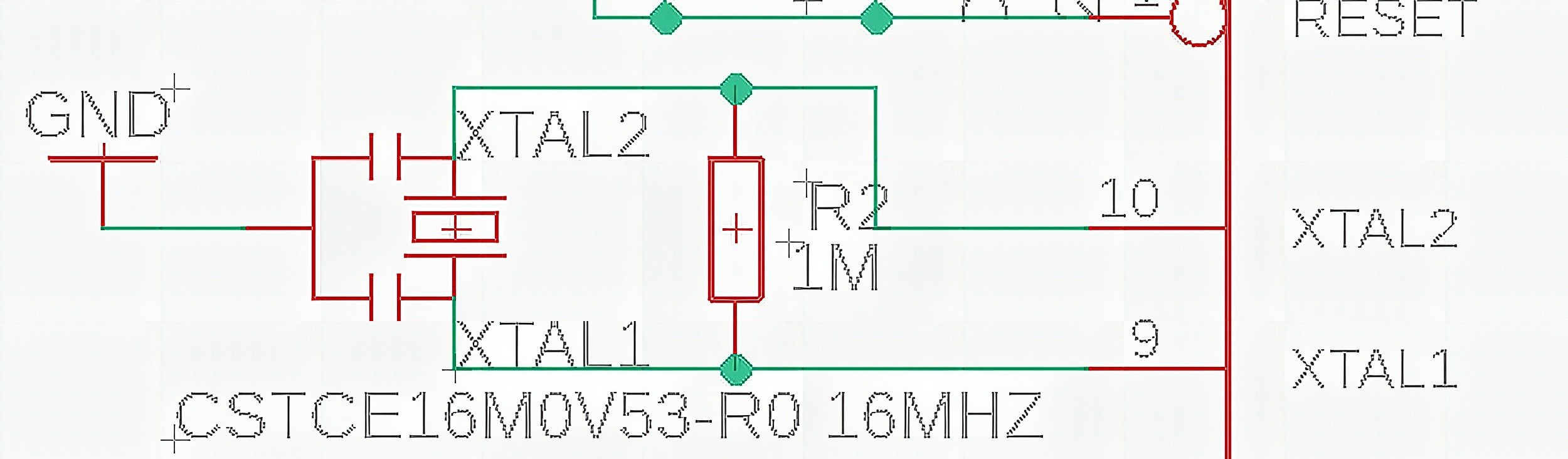
There’s a CSTCE16M0V53-R0 16MHz ceramic resonator connected to the oscillators of the microcontroller. This circuit serves as the clock.
The capacitors here has the same function with the decoupling capacitors in the previous section.
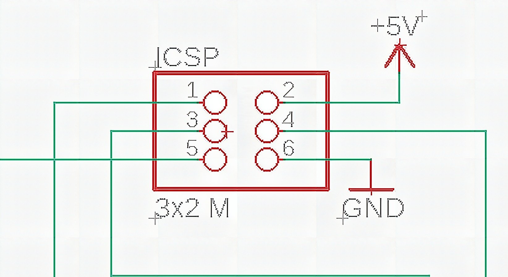
The ICSP (In-Circuit Serial Programming) Header is used to program the ATmega328P using an external programmer ( e.g. Raspberry Pi ). Usually, we only use this for remote programming or for flashing of the microcontroller for the first time. We don’t use this way of programming often since we can already do it via USB, which we will discuss in the next section.
USB

This section is the USB to UART bridge. Since the main microcontroller, ATmega328, does not have a USB transceiver, we use the ATmega16U2 microcontroller as a bridge to translate the USB signals from your computer to UART, the communication protocol the ATmega328 uses.
This is basically the same with the main microcontroller section. This MCU has capacitors, an ICSP header and a crystal as well.

These RN3 resistors are termination resistors. They are used so that the total impedance of the line matches with the USB specification. It slows the speed of the USB pulses lessening EMI interference. On the other hand, Z1 and Z2 are varistors. They are used for ESD (Electrostatic Discharges) protection.

When the ATmega 16U2 transmits or receives a signal from the ATmega 328P, yellow LEDs light up. We can also see here the two lines where the two microcontrollers communicate.
I/O

Quite refreshing to see the board again right? By now, you should be able to appreciate how these are connected to the several electronic components in our schematic diagram. We don’t need to explain them anymore. This is an article for the basic arduino schematic diagram after all.
If you have comments or suggestions, feel free to write below. Get updates on technical articles like this by staying tuned on Learn. I did a test on an TFT LCD previously, you might want to check it out here. Also, I did a tad for the season of gift giving. Check this link if you want to try it out as well. Keep circuit rockin’!
ATmega328P Pin Map: Arduino Pin Numbers vs AVR Ports
The 8-bit ATmega328P uses three I/O ports (B, C, D) but the Uno board labels its headers with friendly numbers (0 – 13 plus A0 – A5). The mapping matters when you write fast code with direct port manipulation, when you read someone else’s pinMode in a hurry, or when you want to understand what the schematic is actually doing.
| Arduino pin | AVR port | Notes |
|---|---|---|
| 0 (RX) | PD0 | UART receive |
| 1 (TX) | PD1 | UART transmit |
| 2 – 7 | PD2 – PD7 | Digital I/O. Pins 2 and 3 also handle external interrupts |
| 8 – 13 | PB0 – PB5 | Pin 11 is MOSI, 12 is MISO, 13 is SCK and the onboard LED |
| A0 – A5 | PC0 – PC5 | Analog input. A4 is also SDA (I2C data), A5 is SCL (clock) |
Reading the schematic you’ll see references like PB5/SCK/PCINT5. Same physical pin (Arduino pin 13) wearing three hats: digital pin, SPI clock, pin-change interrupt source. This is why the LED on pin 13 flickers whenever you transfer over SPI. Not a bug.
USB-to-Serial: 16U2 vs CH340 vs FTDI on Clones
Original Arduino Unos use the ATmega16U2 as the USB bridge. Clones almost always use the CH340 from WCH or sometimes an FT232 from FTDI. They all do the same job (turn USB into a TTL serial stream the ATmega328P can talk to over pins 0 and 1) but they show up differently to your computer.
- 16U2: appears as Arduino Uno in Device Manager. No extra driver needed on Windows 10+.
- CH340: needs the WCH driver on older Windows. On macOS Catalina and newer, it’s already in the kernel.
- FTDI: works out of the box on most systems. Watch for counterfeit FTDI chips that the official driver bricks.
If your board doesn’t show up as a COM port, the USB-to-serial chip is the first thing to suspect. Not the ATmega328P. The 328P never sees the USB at all.
Common Mistakes When Reading the Arduino Schematic
- Mixing up Vin and 5V. Vin is whatever your DC jack is supplying (7 – 12V typical) before it hits the regulator. Touching Vin directly with logic-level peripherals is how you fry sensors.
- Treating GND symbols as separate grounds. They’re all the same net. Schematic designers split them so the diagram reads cleanly across pages.
- Reading the ATmega328P pinout straight from the chip datasheet without translating to Arduino pin numbers. Use the pin map above.
- Ignoring decoupling capacitors. Every chip has them. Skipping them on a prototype board is the most common cause of “it worked yesterday” bugs.
- Forgetting that pin 13 doubles as SPI clock. If you’re using SPI, the onboard LED will blink with every transfer. That’s expected behavior.
Frequently Asked Questions
What does this How to Read the Arduino Schematic Diagram tutorial cover?
Get deeper into the Arduino craft by looking into a reference design.
Can I use an Arduino Nano or Mega instead of UNO for the How to Read the Arduino Schematic Diagram build?
Yes. Nano shares the same ATmega328P and pinout. Mega has more I/O if you outgrow UNO. The code stays the same — just match the pin numbers used in the Sample Code section.
Why does my How to Read the Arduino Schematic Diagram sketch fail to upload?
Usually wrong COM port, missing CH340/CH341 driver for clone boards, or another program holding the serial port. Disconnect the board, install the driver, reselect the port, retry.